Why we use PCB single panel process?
The primary reason for having your boards delivered in an array is to make automated assembly faster and less expensive. Running an array of boards through a pick-and-place machine is far more efficient than sending them through one at a time. Arrays are also desirable because they allow the addition of tooling rails, tooling holes, and fiducials, all of which help your assembler.
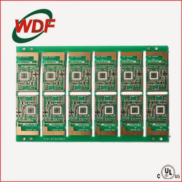
PCB single panel process
Cutting→drilling printed circuit→the entire board gold→etching→inspection and printing solder→tin spraying→printing character→forming and finished product inspection→rosin and packaging
Process HASL process PCB double-faced board
Cutting, drilling, copper deposition, board ( thickened copper ), image transfer, electrical copper tin, tin, inspection and printing etching resistance welding, seal character, spray tin, forming, testing, product inspection and packaging
Process HASL process of PCB multilayer board
Open the material, inner layer, inner layer etching, Inner Inspection and melanization ( brown )→→→→plate laminated shooting drill electric ( thickened copper ), pattern transfer ( outer ), electrical copper tin, tin, inspection and printing etching resistance welding, seal character, spray tin, forming, testing, product inspection and packaging
PCB multilayer board finger + HASL process
Open the material, inner layer, inner layer etching, Inner Inspection and melanization ( brown )→→→→plate laminated shooting drill electric ( thickened copper ), pattern transfer ( outer ), electrical copper tin, tin, inspection and printing etching resistance welding, seal characters, gold finger, spray tin, forming, testing, product inspection and packaging
FPC single panel process:
Cutting, drilling, dry film lamination, counterpoint, exposing, developing, etching, stripping, surface treatment, paste coating and pressing, curing and surface treatment, ENIG, seal characters, cutting, electrical measurement, punching, final inspection, packing and shipment
FPC double-faced board process:
Cutting, drilling→ PTH →plating, pretreatment, dry film lamination, counterpoint, exposing, developing, figure plating, pretreatment, dry film lamination, exposure, developing, etching, stripping, surface treatment, paste coating and pressing, curing and ENIG, seal characters, cutting, electrical measurement→punching, final inspection, packing and shipment of stripping,
Technological process of FPC multilayer board
Open the material, inner layer, inner layer etching, Inner Inspection and melanization ( brown )→→→→laminated targeting drilling deposit copper and board ( thickened copper ), pattern transfer ( outer ), electrical copper tin, tin, inspection and printing etching resistance welding, chemical nickel gold, seal characters, forming to test, product inspection and packaging
Rigid-flex pcb node ( FPC ) plate process
Open the material, inner layer, inner layer etching, Inner Inspection and melanization ( brown )→→→→laminated targeting drilling deposit copper and board ( thickened copper ), pattern transfer ( outer ), electrical copper tin, tin, inspection and printing etching resistance welding, chemical nickel gold, seal characters, forming to test, product inspection and packaging.